
Review D: Components of digital circuits: Questions
Draw two truth tables illustrating the outputs of a half-adder, one table for the sum output and the other for the carry output.
Fill in the truth table at right for the following circuit. Ignore rows not included in the table.

a b c x y 0 1 1 1 0 1 1 1 0 1 1 1
In terms of the meanings of inputs and outputs, what distinguishes a half adder from a full adder?
Using only half-adders, diagram how you could construct a full adder. Be sure to label your inputs x, y, and z and the outputs carry and sum. Also, please label the outputs carry and sum for each half-adder.
Using only half adders and full adders, diagram a circuit that takes six inputs representing two 3-bit unsigned binary numbers a2a1a0 and b2b1b0, and which produces an output of a 4-bit result s3s2s1s0 representing the sum of the two numbers. Label your input and output wires.
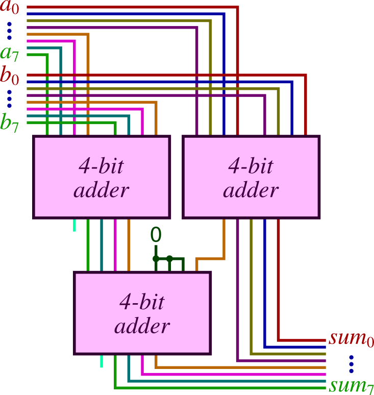
Using only four-bit adders, construct an eight-bit adder. Each four-bit adder has two four-bit inputs and one five-bit output. Your eight-bit adder should have two eight-bit inputs and a one eight-bit output (don't worry about the ninth output bit).
Suppose we have a 4-to-1 multiplexer whose inputs are d00, d01, d10, d11, s0, and s1. What is the output in each of the following cases?
| d00 | d01 | d10 | d11 | s0 | s1 | out |
| 0 | 0 | 0 | 0 | 1 | 0 | |
| 0 | 0 | 0 | 1 | 1 | 1 | |
| 0 | 0 | 1 | 0 | 0 | 0 | |
| 0 | 1 | 0 | 1 | 1 | 0 | |
| 0 | 1 | 1 | 1 | 1 | 1 | |
| 1 | 1 | 0 | 1 | 0 | 1 | |
| 1 | 1 | 1 | 0 | 1 | 1 |
Describe the inputs and outputs of a 1-to-4 demultiplexer, and how they relate.
For the following circuit using two 2-to-1 multiplexers, complete the corresponding truth table.

Using only 2-to-1 multiplexers, build a 4-to-1 multiplexer. You should label your circuit's inputs d00, d01, d10, d11, s0, and s1, and you should label the circuit's output out.
Draw a circuit taking two 2-bit inputs a and b (whose individual bits are a1a0 and b1b0) as well as a 1-bit input op. The output of the circuit should be a 3-bit number that is a + a if op is 0 and a + b if op is 1.
Feel free to use components we saw in class, such as adders, multiplexers, demultiplexers, and flip-flops.
Some circuits are combinational, while others are sequential. What distinguishes these two types of circuits?
Draw an S-R latch using NOR gates. Label the S and R inputs and the Q output so that R, when 1, resets the latch value to 0, and S, when 1, sets the latch value to 1.
Describe the distinction between the behavior of an edge-triggered component (as with a D flip-flop) and a level-triggered component (as with a D latch).
Explain how the below implementation of a D flip-flop creates an edge-triggered circuit out of two level-triggered D latches.

Recall that a D flip-flop as studied in class takes two inputs, D and ck, and it has an output named Q. Suppose all inputs and the output are currently 0, and the inputs change as described below. When does Q change within the event sequence, and to what value?
| 1. | D changes to 1. |
| 2. | ck changes to 1. |
| 3. | D changes to 0. |
| 4. | ck changes to 0. |
| 5. | ck changes to 1. |
| 6. | D changes to 1. |
The below circuit includes two D flip-flops. Recall that a D flip-flop's stored state remains unchanged as long as set = 0. At the instant that set switches to 1, its stored bit switches to value, and it retains this value until set changes to 1 again.

Say a user enters the sequence of inputs given in the table at right, one after the other. Label what the output of the circuit will settle into after each of the user's inputs.
a b c o 1 1 1 ? 0 1 1 ? 0 0 1 ? 0 0 0 ? 0 1 0 ? 0 0 0 ? 1 0 0 ?
Suppose the upper D flip-flop in the below circuit were holding 1 and the lower D flip-flop held 0, while the x input were 0. Then somebody toggles the x input five times (to 1, then 0, then 1, then 0, then 1). Complete the table to show how the output values would change.

x a b 0 1 0 1 0 1 0 1
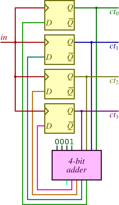
We studied the below circuit implementing a counter for a turnstile. How would this circuit behave if we were to use D latches (level-triggered) in place of the D flip-flops (edge-triggered)?
Using a 2-to-1 multiplexer and a D flip-flop, build a circuit that has one output and three inputs T, X, and ck. The circuit's output should stay at the same value regardless of the inputs, until the instant when ck changes from 0 to 1. At that time, if T is 1, the circuit's output should toggle to its opposite value; and if T is 0, the output should change to the value of X at that instant.
Note: Do not use logic gates. Recall that a D flip-flop has outputs Q and Q.
Using two D flip-flops and simple logic gates (AND/OR/NOT), build a circuit whose output is 1 on every fourth clock cycle. That is, when the output is 1, the output should flip to 0 for the next three times the clock goes from 0 to 1, then flip to 1 for the fourth time, then repeating the cycle.
Using just AND, OR, and NOT gates in addition to two D flip-flops, build a single-input circuit whose two-bit output changes as follows each time its single input rises from 0 to 1: When the output is 01(2), it changes to 10(2); when the output is 10(2), it changes to 11(2); and when the output is 11(2), it changes to 01(2). (This might be useful for controlling a traffic light.)
Suppose I have eight flip-flops numbered 0 through 7 and I have a 3-bit memory address indicating which flip-flop's bit I wish to retrieve. What component would be useful for retrieving the bit from the appropriate flip-flop?
Review D: Components of digital circuits: Solutions
|
|
| a | b | c | x | y |
| 0 | 1 | 1 | 1 | 0 |
| 1 | 0 | 1 | 1 | 1 |
| 1 | 1 | 0 | 1 | 1 |
| 1 | 1 | 1 | 0 | 0 |
A half adder has two inputs and outputs the sum of these two bits, while a full adder has three inputs and outputs the sum of these three bits.


The design of this circuit is similar in structure to the design of a full adder using half adders.
| d00 | d01 | d10 | d11 | s0 | s1 | out |
| 0 | 0 | 0 | 0 | 1 | 0 | 0 |
| 0 | 0 | 0 | 1 | 1 | 1 | 1 |
| 0 | 0 | 1 | 0 | 0 | 0 | 0 |
| 0 | 1 | 0 | 1 | 1 | 0 | 0 |
| 0 | 1 | 1 | 1 | 1 | 1 | 1 |
| 1 | 1 | 0 | 1 | 0 | 1 | 1 |
| 1 | 1 | 1 | 0 | 1 | 1 | 0 |
A 1-to-4 demultiplexer has three inputs, including a data input and two select inputs representing the two bits of a number s. It has four outputs, number 00(2) through 11(2). The demultiplexer routes its data input to the output whose number is s; the other outputs' values will be 0.
| x | y | out |
| 0 | 0 | 0 |
| 0 | 1 | 0 |
| 1 | 0 | 1 |
| 1 | 1 | 1 |


In a combinational circuit, the output can be determined entirely by the current combination of inputs. In a sequential circuit, the output may also depend on the sequence of previous inputs.

In an edge-triggered device, the value changes only at that instant that the clock input becomes 1. In a level-triggered device, however, the memory value continues adopting any values given as long as its set input is 1. (For example, in a D flip-flop, if the D input changes while clock remains 1, the remembered value doesn't change. In a latch, however, the D input changing while set is 1 results in a change to the remembered value.)
As long as ck is 0, the second latch's set input is 0, so its value and its output remains unchanged. For the first latch, though, the set input is 1, and so the first latch's value continuously updates to the value of D. When ck changes to 1, the first latch's set input changes to 0, so the latch's value freezes at the value of D at the time that ck changed to 1. Meanwhile, when ck becomes 1, the second latch's set input changes to 1, and so it begins setting the latch's value to its data input — which is the value of D at the time that ck became 1 as stored in the first latch.
At step 2, the D flip-flop's value changes to 1. At step 5, it changes to 0.
| a | b | c | o |
| 1 | 1 | 1 | 1 |
| 0 | 1 | 1 | 1 |
| 0 | 0 | 1 | 1 |
| 0 | 0 | 0 | 1 |
| 0 | 1 | 0 | 0 |
| 0 | 0 | 0 | 0 |
| 1 | 0 | 0 | 1 |
| x | a | b |
| 0 | 1 | 0 |
| 1 | 0 | 0 |
| 0 | 0 | 0 |
| 1 | 0 | 1 |
| 0 | 0 | 1 |
| 1 | 1 | 0 |
For the duration that somebody is in the beam (in is 1), the latches will update their data inputs. The new values will feed into the adder, which will feed back into data inputs, for updating the latches again, and again, and again. The consequence is that the counter counts as quickly as it can as long as somebody is in the beam; once the person exits the beam, the resulting value has gone up by far more than 1, increasing by an unpredictable amount.
(Actually, since the different adder outputs have different depths, and since there will inevitably be variations in how fast the transistors update anyway, the behavior is even more erratic than simply counting very quickly: Some latches will update more frequently than other latches.)


We would want an 8:1 multiplexer, where each flip-flop's output is wired into one of the multiplexer's indexed inputs, and the address bits are connected to the multiplexer's select inputs.