Components of digital circuits
by Carl Burch, Hendrix College, September 2011
Components of digital circuits by Carl Burch is licensed under a Creative Commons Attribution-Share Alike 3.0 United States License.
Based on a work at www.cburch.com/books/comps/.
Contents
1.1. Half adder
1.2. Full adder
1.3. Multibit adder
2. Components for routing
2.1. Multiplexer
2.2. Demultiplexer
3. Components for remembering
3.1. SR latch
3.2. D latch
3.3. D flip-flop
3.4. JK flip-flop
4. Sequential circuits
4.1. Counter
4.2. Register
4.3. Memory
While logic gates are the essential foundation to working circuits, ultimately a single logic gate does very little. It's also handy for our toolbox to include pieces that perform more complex operations. We call these more complex pieces components, and studying them is important to understanding computational circuits.
In this document, we'll learn about three particularly important categories of components: adding components, routing components, and memory components.
1. Components for adding
We'll start with components for adding binary numbers together.
1.1. Half adder
Let's begin the discussion by considering the basic adding process — how would we add two numbers? Of course, you already know how to add base-10 numbers from your studies in grade school: You start from the rightmost column (the 1's digits), add them together, write the result in the rightmost column of the result and possibly carry a 1 into the next column. You proceed column by column, leftward.
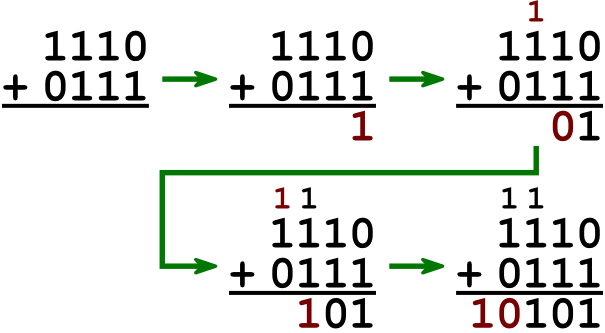
We can add binary numbers using a similar approach. The illustration below shows of the process of adding the two four-bit numbers 1110(2) = 14(10) and 0111(2) = 7(10).
We'll want to build a circuit that follows this process. For the moment, let's worry about just the first step: adding the rightmost bit from each number. What we'll want is a circuit that takes two input bits — we'll call them a and b — and computes the sum of these two bits. Since the sum could possibly be a two-bit number, this circuit will have two outputs: sum will be the sum's 1's-bit, and cout will be the sum's 2's-bit. We'll call this circuit a half adder.
We can design our half adder circuit by building a truth table that enumerates each possible combination of the two inputs along with the appropriate value for cout and sum in each case.
a b cout sum 0 0 0 0 0 1 0 1 1 0 0 1 1 1 1 0
To interpret this table, let's look at the last row, where a and b are both 1. In this case the output is based on the sum of 1 and 1, which is 10(2). We'd place the 1's bit of this sum (which is 0) into the bottom of the rightmost column, so this row of the truth table says that sum should be 0. And we'd carry the two's bit of the sum (which is 1) into the next column, so the truth table says that cout should be 1.
To build a circuit corresponding to this truth table, we need to determine how each output relates to its inputs. We first notice that the cout output is the AND function on a and b. The sum output, on the other hand, is 1 if a is 1 or b is 1, but not both. This is the exclusive-or function on a and b; it is often abbreviated as the XOR of a and b. We draw a XOR gate as an OR gate with a shield on its inputs.

However, if we insist on drawing the circuit with just AND, OR, and NOT gates, we can derive the sum-of-products expression for sum: a b + a b. The resulting circuit is equivalent to the XOR gate.
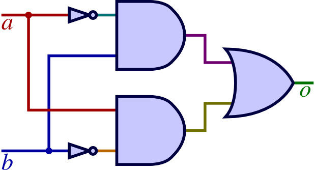
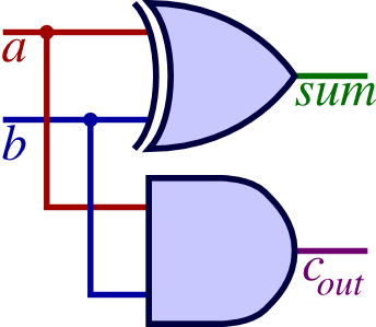
With a XOR gate built, we can now put together our half adder: sum will be the exclusive OR of a and b, while cout will be the AND of a and b.
We'll employ this circuit in other circuits that we build.
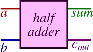
Even though the diagram is rather simple, we'll
prefer instead to draw an even simpler box labeled half
adder
to represent this circuit:
1.2. Full adder
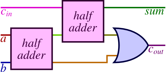
Now let's consider the subsequent steps in our addition procedure, where we add later columns. In each of these later columns, there is a possibility that we have a carry coming in from the preceding column. Thus, we'll now want to build a circuit with three input bits and produces the sum of these inputs as its output. We'll use a and b to represent the bit from each of the numbers in the column; but there will be a third input which we'll call cin corresponding to the potential carry from the preceding column. Our circuit will again have two output bits, since the sum of three 0/1 values can be a two-bit output; the bit placed as the result for the column will again be called sum, and the number carried into the next column will again be cout.
We've already seen how we to build a circuit for adding the two input bits a and b together: We can simply use a half adder for that. But we also want to add cin to this sum. To accomplish this, we can use an additional half adder, whose inputs would be the sum from the first half adder and cin.
But we'll be left with two values of cout from these two half adders. What should we do to them? We essentially want to add them together, so we could use yet another half adder to accomplish that. But in fact we can guarantee that at least one of these two cout values will be 0: After all, if cout happens to be 1 from the first half adder, then that half adder's sum output must necessarily be 0 — and with a 0 as one of the inputs into the second half adder, its cout would be 0. Since at most one of these cout values will be 1, we can add them together using a simple OR gate. That's a better choice than a third full adder because it requires fewer gates.
This leads to the following circuit.
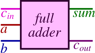
As with the half adder, we'll want to reuse this circuit
again. We'll feel free to draw a box labeled
full adder
that represents this circuit.
1.3. Multibit adder
Now we can put these pieces together to build an adder for two multibit numbers. For the moment, we'll imagine that we want to build a circuit for adding two four-bit numbers, a and b. The a input (and the b input) will actually come into our circuit through four wires; we'll label the 1's bit of a as the a0 wire, the 2's bit the a1 wire, the 4's bit the a2 wire, and the 8's bit the a3 wire. (The system here is that ai corresponds to the 2i's bit from a.) We'll similarly do the same thing for b and for our output sum which will in fact be five wires, since the sum of two four-bit numbers may be a five-bit number (for example, 1111(2) + 1111(2) is 11110(2)).
To build our complete circuit, we'll use a half adder to add the 1's bits a0 and b0. Then we'll use a full adder to add the 2's bits a1 and b1 along with the carry from the preceding column. And we'll continue with full adders, so that our complete four-bit adder is wired as follows.

2. Components for routing
In building more complex circuits, one often wants an analogy
to an if statement: You want
signals to be routed in one way or another depending on the
value from another wire. For this, we will want
multiplexers and demultiplexers, which we
study in this section.
2.1. Multiplexer
The multiplexer is a circuit whose output is
one of several inputs, depending on the value given by some
other selection
inputs. In a circuit, a multiplexer is
drawn as a trapezoid as follows.
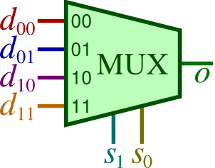
This is a 4-to-1 multiplexer. On the left side, you
can see four data
inputs, which we'll call
d00,
d01,
d10, and
d11.
On the bottom, you can see two selection
inputs, which we'll call
s1 and
s0.
And on the right, you can see the multiplexer's output.
What does a multiplexer do? It routes one of the data inputs to the multiplexer's output; which of the data inputs goes out is determined based on the select inputs. For example, if s1 is 1 and s0 is 0, then the d10 input is routed to the output. If instead s1 is 0 and s0 is 1, then the circuit's output would be d01 instead. It's helpful to think of this a multiplexer as a railroad switch, connecting one input to an output; the selection inputs control the angle of the switch.
While a railroad switch is helpful in thinking about how a multiplexer works, circuits don't actually have moving parts. If we're going to build a multiplexer, then we can only use wires and logic gates to build it. Our solution will be to include an AND gate for each of the data inputs, and to have each of the AND gates feed into an OR gate. The AND gate corresponding to a data input will be 0 whenever the selection inputs don't correspond to the data input; that way, the AND gate corresponding to an unselected data input doesn't affect the OR gate's output, and so the OR gate's output will match the output of the AND gate whose data input is selected. We include the data input on each corresponding AND gate so that this AND gate's output will match the data input when that data input is selected. Here's the circuit diagram.
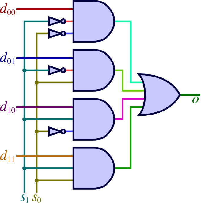
This particular multiplexer is a 4-to-1 multiplexer, so called because it routes one of four inputs to a single output. Other common multiplexer ratios are 2-to-1, which would have one selection bit; 8-to-1, with three selection bits; a 16-to-1, with four selection bits; and even 32-to-1, with five selection bits.
2.2. Demultiplexer
The demultiplexer reverses the process of a multiplexer: It routes a single input into one of several outputs, while the unselected outputs should emit a value of 0. We represent it in a larger circuit as follows.
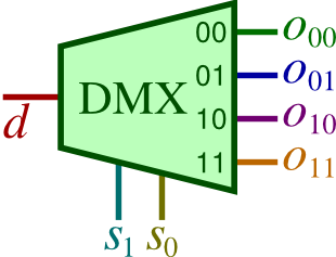
Internally, its circuit is similar to that of a multiplexer's, though it is simpler because each output is treated independently. Below is an implementation diagram.
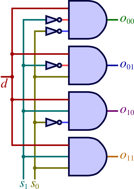
This is a 1-to-4 demultiplexer. Other common ratios are 1-to-2, 1-to-8, 1-to-16, and 1-to-32; the number of selection bits will vary depending on how many are required to indicate which output to use.
3. Components for remembering
So far, all the circuits we've build have been combinational circuits: An output is determined purely by the current combination of inputs. We've built several useful combinational circuits, but it can also be useful for a circuit's behavior to depend on previous inputs. Such circuits where the sequence of previous inputs also matters are called sequential circuits. And to build sequential circuits, we'll want memory, so in this section we'll examine one-bit memories called latches and flip-flops.
3.1. SR latch
We begin by considering the following little circuit, which uses two NOR gates. Each NOR gate behaves as an OR followed by a NOT gate: Given the inputs a and b, a NOR gate's output is the value a + b.
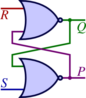
This circuit has each NOR gate's output going into the input of the other NOR gate, essentially forming a figure-eight loop. This is peculiar: We haven't seen a circuit with such loops before. But it is this loop that gives rise to our memory.
So what does this circuit do? Let's see what happens with a particular sequence of inputs:
| Inputs | Description | Outputs | |
| a. | R = 1, S = 0 | The upper gate has a 1 input, and 1 OR anything is 1, so the upper gate's output Q is 0. This 0 wraps around to the lower gate, whose inputs are 0 and 0, so the lower gate's output P is 1. | Q = 0, P = 1 |
| b. | R = 0, S = 0 | With R changing to 0, the upper gate still sees a 1 coming from the lower gate, so its output Q remains at 0; thus, the upper gate's inputs have not changed. And neither input to the lower gate has changed, so its output doesn't change either. | Q = 0, P = 1 |
| c. | R = 0, S = 1 | With S changing to 1, the lower gate's output P changes to 0. This wraps around to the upper gate, which sees inputs of 0 and 0, so its output Q changes to 1. This wraps around to the lower gate so that the lower gate sees 1 and 1, but its output P remains at 0. | Q = 1, P = 0 |
| d. | R = 0, S = 0 | With S changing back to 0, the lower gate still receives a 1 from Q, so its output P remains at 0. The upper gate's inputs have not changed, so its output Q remains at 1. | Q = 1, P = 0 |
| e. | R = 1, S = 0 | With R changing to 1, the upper gate's output Q becomes 0. This wraps around to the lower gate's input, which sees two 0 inputs, and so its output P is 1. | Q = 0, P = 1 |
Below is a timing diagram summarizing this sequence of events. A timing diagram has a row for each of various points in the circuit, with a line showing how the voltage at each point changes over time. (The 0/1 numbers that you see here would be omitted from a traditional timing diagram.) Time increases as we go to the right. For example, we can see that at point R in the circuit, the value is initially 1, but then it changes to 0 for time b and stays there until changing back to 1 at time e.

(Incidentally, you might notice some anomalies in our timing diagram that aren't really important for our discussion here. First, each change in Q and P lags slightly behind a change to R or S. This is because there's a slight delay while a NOR gate responds to a change in its inputs. Also, the transitions between 0 and 1 aren't perfectly vertical lines. This is because we're actually talking about voltages, which are continuous, so the voltage cannot shift from 0 to 1 instantaneously as a vertical line would imply.)
Notice that at times b and d, the inputs to the circuit are the same — both R and S are 0 — but the output values Q and P are different! The difference between these situations is what the values of Q and P were previously. When both inputs are 0, Q and P remain unchanged from what they were previously. This is what gives this little circuit memory.
The following table summarizes how different R-S inputs affect Q.
R S new Q 0 0 old Q 0 1 1 1 0 0 1 1 avoid
We haven't accounted for the final row, where both inputs are 1. We'll simply avoid this situation altogether: It leads to both P and Q being 0, and we would like to maintain the fact that P and Q are always opposing values.
Notice from our timing diagram, though, that as long as we avoid this situation, P is consistently the opposite of Q. For this reason, our subsequent discussion will label this output Q rather than as P.
This circuit is called an SR latch.
It's called a latch because it has the ability to
lock in
a bit (when the two inputs are both 0).
The SR
part of the name comes from the names of the inputs.
We use the letter S for one input because when that
input is 1 (and the other input is 0), the remembered
bit is Set to 1. Likewise, we use the letter R
for the other input because when that bit is 1 (and the other
input is 0), the remembered bit is Reset to 0.
3.2. D latch
While the SR latch is handy, it would be even nicer if we had a latch whose inputs were more convenient: We'd like one input to indicate when the latch's value should update, while the other input indicates what the new value should be. We'll call such a circuit a D latch: The D designation stands for the Data input that carries the latch's new value.
We'll call the first input set and the second input data. When set is 0, the circuit should do nothing except continue emitting what it remembers. But when set becomes 1, the circuit should begin remembering data's value instead. Thus, we would hope that the circuit works as illustrated by the below table.
set data new Q 0 0 old Q 0 1 old Q 1 0 0 1 1 1
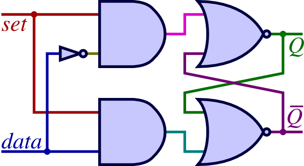
We can build a D latch using an SR latch. We'll start by correlating each combination of set/data inputs to an R/S combination from the SR latch. For example, when set and data are both 0, we want the remembered bit Q to remain unchanged; to do this using the SR latch, we'd want R and S both to be 0. Or to take another example: When set and data are both 1, we want the remembered bit Q to become 1; to do this using the SR latch, we'd want R to be 0 and S to be 1. We can build up a table summarizing this and the other two set/data combinations.
set data new Q R S 0 0 old Q 0 0 0 1 old Q 0 0 1 0 0 1 0 1 1 1 0 1
Based on this table, we can determine that R should be set ⋅ data, while S should be set ⋅ data. We use these expressions to build a circuit giving our desired D latch behavior.
3.3. D flip-flop
Latches give us the ability to remember a bit, but its value is subject to change over a relatively long time window — i.e., as long as the set input is 1. In practice, it's more convenient to have a component where this window of change is instantaneous. This allows the remembered value to propagate through the circuit to compute the next value that should be stored in the latch, without a danger of this new value getting back to the latch before the window ends.
To give our latch an instantaneous-update property, we'll look for a latch that updates only at the instant that its set input changes. Such a component is said to be edge-triggered, and the edge-triggered input is often called its clock input. In this document, we examine flip-flops that update when the clock input changes from 0 to 1; these are called positive edges. Circuit designers sometimes instead talk about flip-flops triggered by the clock input changing from 1 to 0; such changes are called negative edges. In the case of a bit memory, we call edge-triggered memories a flip-flop rather than a latch.
A flip-flop's edge-triggered behavior is illustrated by the following timing diagram.

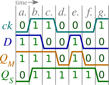
You can see that the clock signal ck changes from 0 to 1 going into time b and time g. At each of these times, the remembered bit Q changes. At time b, the input D is 1, so that's the value that Q becomes. And at time g, D is 0, so Q changes to 0. In between b and g, D changes, but these changes have no effect on Q: The only time Q will change is when ck changes from 0 to 1.
The following circuit implements this idea using a master-slave flip-flop. It uses two D latches; the first is called the master, while the second is called the slave.
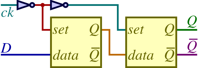
The idea here is that as long as ck is 0, the set input into the master latch will be 1, and so the master latch will update to the current value of D. When ck changes to 1, though, the set input to the slave latch becomes 1, and so it receives the current value of the master latch, which will be the current value of D at that time. At the same time, the set input to the master latch changes to 0, so later updates to D will not have any effect on the master latch's remembered value, and so the slave latch will continue to hold the value of D at the time ck changed from 0 to 1. This process is summarized by the following timing diagram, which includes QM to represent the value remembered by the master latch (the first one) and QS to represent the value remembered by the slave latch (the second one).
In circuit diagrams, we represent the D flip-flop as follows.
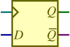
The triangle is a traditional way of denoting edge-triggered inputs — that is, inputs that are only effective when they change.
3.4. JK flip-flop
Besides D flip-flops, there are a few other popular designs for flip-flops. One of the most popular variations is the JK flip-flop. It has three inputs called J, K, and the clock.
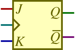
As a flip-flop, the value of its remembered bit Q changes at each instant that the clock input changes from 0 to 1 (or from 1 to 0 if it is a negative-edge-triggered flip-flop). At each such instant, the update to Q depends on the current values of J and K, as given in the below table.
J K new Q 0 0 old Q 0 1 0 1 0 1 1 1 old Q
This table is similar to the SR latch's table, but there are two major differences. First, as a flip-flop, a JK flip-flop's remembered bit changes only at the instant when the clock changes from 0 to 1. And second, the final row is different: With an SR latch, we avoid the case both R and S are 1; with the JK flip-flop, the flip-flop's state toggles when J and K are both 1 at the time that the clock's edge is reached.
Incidentally, the name of the J input comes from the fact that Q Jumps up to 1 when J is 1 (but K is 0); and the name of the K input comes from the fact that Q is Killed down to 0 when K is 1 (but J is 0).
4. Sequential circuits
Having now the essential ability to remember a bit in a circuit using a latch or a flip-flop, we can build sequential circuits that use them.
4.1. Counter
Let's start with a circuit that counts how many times the user has given it a 1 bit as an input. Such a simple circuit would be useful, for example, in a turnstile to count people entering. To do this, we'll use four flip-flops to remember the current count in binary. (Our counter will only count up to 15, the largest four-bit number, and then it will reset to 0. If we want to count higher, we would need more flip-flops.) And we'll include a four-bit adder to compute the next value for these four flip-flops, as seen in the circuit diagram below.
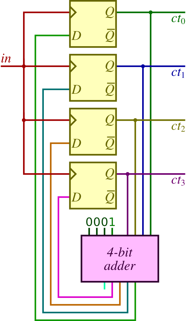
To get a feel for how this circuit works, suppose the in input is 0, and all the D flip-flops hold 0. These outputs feed into the four-bit adder, which also takes its other input of 0001(2), and its output is 0000(2) + 0001(2) = 00001(2). The lower four bits of this output are fed into the D flip-flops' D inputs, but the flip-flops' values don't change, because their clock inputs (wired to in) are all 0. (The upper bit of the adder's output is ignored — in the circuit, we acknowledge this by leaving that output unconnected.)
When the in input changes to 1, then the flip-flops' values will suddenly change their remembered values to match their current D inputs. In this case, the four D inputs are 0001, so these are the bits remembered by the flip-flops, and that becomes the overall circuit's output. At the same time, the four-bit adder would also receive these newly remembered values, so that the adder would output 0001(2) + 0001(2) = 00010(2). This sum is fed back into the flip-flops' D inputs, but the flip-flops values won't change yet, because flip-flops change their value only at the instant that in becomes 1, and that time has long past before 0010(2) reaches them. The flip-flop values won't update to 0010 until the in input goes down to 0 and back up to 1 again.
This last point, by the way, illustrates the advantage of flip-flops over latches. Suppose we used latches instead. Because the set input would still be 1 at this point, the latches would begin remembering 0010(2). And this would go through the adder, and the 0011(2) would go into the latches. This would go through the adder, and 0100(2) would go into the latches. The circuit would count incredibly fast as long as set remains at 1, and we wouldn't be able to predict where it would stop once set goes back to 0. (In fact, it is more complex than that, because gates aren't all identically fast, and the adder's circuit doesn't have the same depth for each output, and the wires aren't identically long. Thus, the changes in latches' values would be more erratic.) Using flip-flops, however, the count goes up only once each time the input goes to 1.
4.2. Register
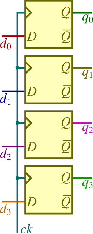
A register is a component for remembering several related bits. The following is a diagram of a four-bit register.

The outputs on the right continually emit the current contents of the register. The clock input, represented with a small triangle on the component's lower edge, tells the register when to alter its value. When this input changes from 0 to 1, the register changes its remembered bits to the values existing on the data bits on the register's left side.
Building a register is a straightforward task: It's just a matter of putting several D flip-flops together, sharing the same ck input, as in the below diagram of a four-bit register's internals.
4.3. Memory
The final sequential circuit we'll consider is a random-access memory, which stores several pieces of information indexed by addresses. We'll access the memory using the following inputs and outputs:
- A multibit input addr, which selects which of the memory locations we are accessing. If this is 10 bits long, it allows us to access 1,024 different memory locations.
- A multibit output out, which indicates the value at the memory location supplied by the addr input. The number of bits in this output will correspond to the size of each individual memory location.
- A one-bit input ck, which indicates that a value should be saved into the memory location supplied by the addr input whenever ck transitions from 0 to 1.
- A multibit input in, which indicates what value should be written into memory whenever ck transitions from 0 to 1. The number of bits in this input will correspond to the size of each individual memory location.
This circuit would be too large to draw even for a small memory of 32 bytes. For the sake of keeping the circuit manageable, we will have to restrict ourselves to just a 4-bit memory, which is enough to illustrate the basic concepts. This 4-bit memory will have its four memory locations indexed by the binary numbers 00, 01, 10, 11, and so the addr input will be 2 bits long. The in input and out output will be just a single wire each, since each memory location holds only one bit.
Our implementation will include four D flip-flops, corresponding to each of the four bits of memory. We will employ a demultiplexer and a multiplexer to route in and out to the flip-flop identified by the current addr input. You can also see that each flip-flop has its own 2-to-1 multiplexer.
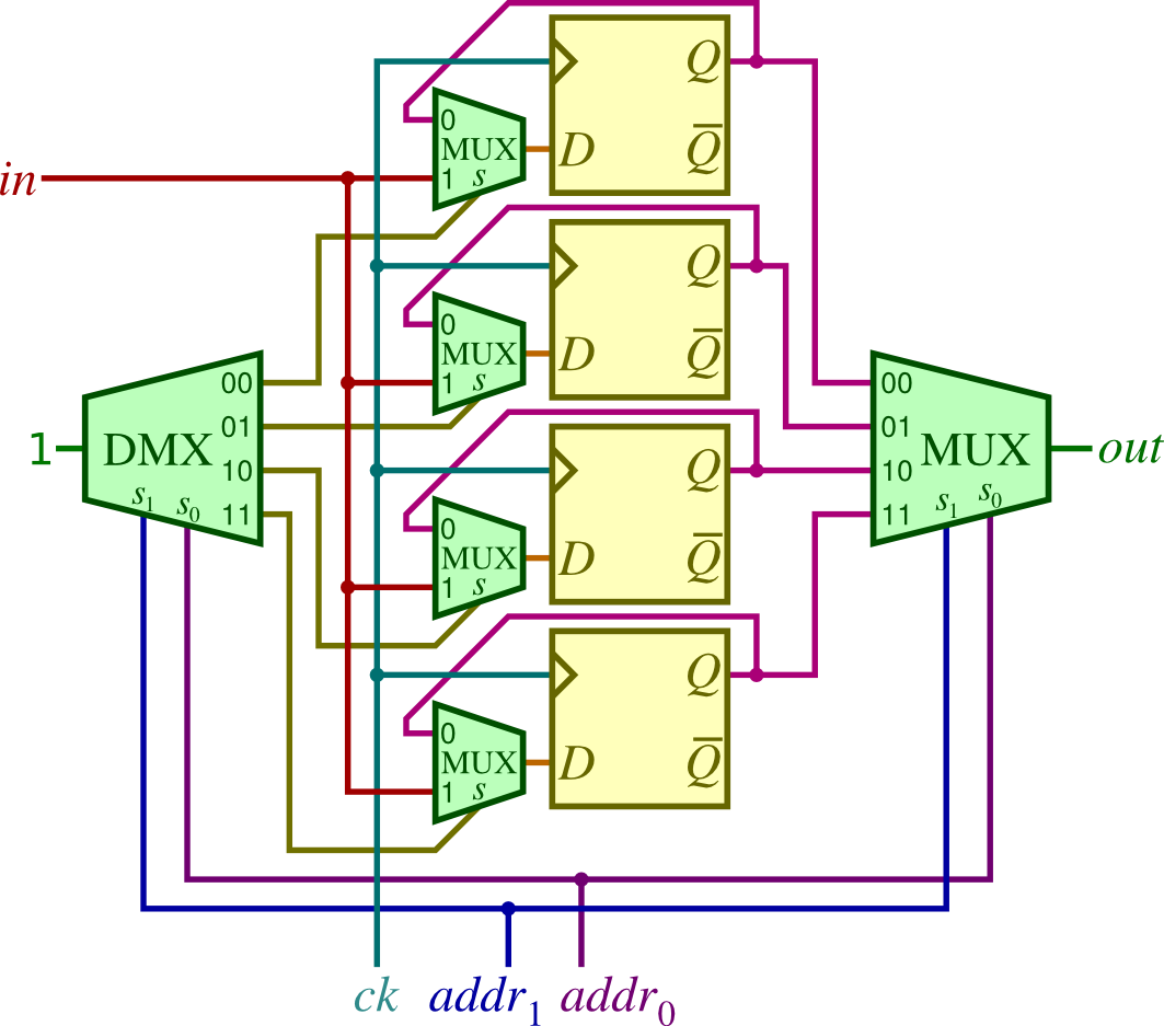
The easy part of this circuit is the right-hand side for reading a value from the selected flip-flop to be out. We send each of the flip-flops' values into a 4-to-1 multiplexer, and we use addr to select which of these the multiplexer should send into the out output.
The part on the left side, which stores in into the selected flip-flop, is more complex. Each of the flip-flops has its D input coming from a 2-to-1 multiplexer. This small multiplexer will route either the flip-flop's current value (if s is 0) or the value of the in input (if s is 1). The 1-to-4 demultiplexer will send 1 to the s input of the 2-to-1 multiplexer identified by the addr input, so that this flip-flop is the only one that sees the in input; the other 2-to-1 multiplexers would receive 0 for the s input, so they would see just the flip-flop's current value. When ck changes from 0 to 1, all flip-flops update (since ck is wired to the clock of all flip-flops), but the ones that aren't indicated by addr will simply update to the same value that they already held, since s is 0 for each of these flip-flop's 2-to-1 multiplexers. The one that is indicated by addr would see the value of in on its D input, so it would update to this value.
To inflate this into a 32-bit memory, we would need to add more flip-flops and 2-to-1 multiplexers, and we would replace our 1-to-4 demultiplexer and 4-to-1 multiplexer with a 1-to-32 demultiplexer and 32-to-1 multiplexer. To change this memory to hold 32 bytes instead of 32 bits, we would duplicate this circuit into eight copies, sharing the same address bits and set bit but using different input and output bits. Such a circuit ends up being quite large.
In real life, by the way, the RAM that one purchases and installs in a computer is implemented in a very different way: A common technique is to use an electrical capacitor for each bit, which can hold an electrical charge for a brief moment. Since capacitors quickly lose their charge, this necessitates frequent recharging. This design leads to much electrical complexity, but it requires less circuit space, so that more bits can be stored in a single chip. The details of this are beyond the scope of this book.
But the above circuit using flip-flops is still useful, because using D flip-flops is the fastest known technique for implementing memories. Unfortunately, it is also quite expensive. Thus, modern computers will use capacitor-based RAM for the bulk of memory, but they use D flip-flops as in the above circuit to construct a small cache for holding the memory that is accessed most frequently.