Logic & circuits
by Carl Burch, Hendrix College, September 2011
Logic & circuits by Carl Burch is licensed under a Creative Commons Attribution-Share Alike 3.0 United States License.
Based on a work at www.cburch.com/books/logic/.
Contents
2. Building logic circuits
2.1. Boolean expressions
2.2. Boolean algebra laws
2.3. Sum of products
3. Simplifying circuits
3.1. Measuring circuit efficiency
3.2. Karnaugh maps
3.3. A more complex Karnaugh map
4. Other logic gates and universality
To understand how computers work, we will want to understand the fundamentals of digital circuits. As it turns out, digital circuits are built on the foundation of basic logic.
1. Logic circuits
At the most basic level, of course, a computer is an electrical circuit build using wires. We'll think of each wire in the circuit as carrying a single information element, called a bit. The word bit comes from Binary digIT, using the term binary because a bit can have either of two possible values, 0 and 1. In electrical terms, you can think of zero volts representing 0 and five volts representing 1; but for our purposes, the specific voltages aren't important — and indeed there are varying systems for interpreting voltage levels as 0 or 1. (People have experimented with more than two different voltage levels, but this ends up leading to circuits that are more complex and end up being less effective than the binary system.)
Here is an example showing the diagram of a simple logic circuit.
Figure 1: A simple logic circuit.
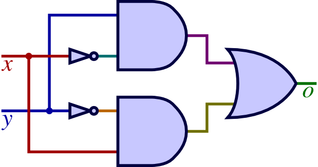
This diagram consists of some peculiar shapes connected with some lines. The lines represent wires; the shapes represent what are called logic gates, which we'll study soon.
We'll think of each wire as carrying a bit until it hits a gate. You can see that some wires intersect in a small, solid circle: This circle indicates that the wires are connected, and so values coming into the circle continue down all the wires connected to the circle. If two wires intersect with no circle, this means that one wire goes over the other, like an Interstate overpass, and a value on one wire has no influence on the other.
(In our circuits, we'll draw systems of wires using different colors, so you can tell that two wires don't touch when you see them in different colors. Traditionally, though, circuits are drawn using black and white only, and these dots are crucial for understanding when wires intersect and when they overlap.)
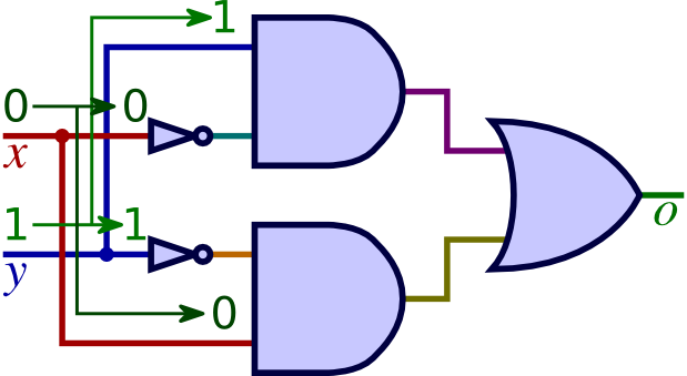
Suppose that we take our example circuit from Figure 1 and send a 0 bit on the upper input (x) and a 1 bit on the lower input (y). Then these inputs would travel down the wires until they hit a logic gate.
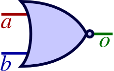
So what happens when an input reaches a logic gate? It depends on what type of logic gate it is. There are three major types of logic gates, depicted using three different shapes.
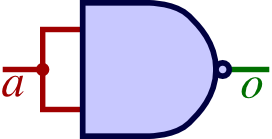
| NOT gate: | Takes a single bit on its left and produces the opposite bit on its right (Figure 2(a)). For the upper NOT gate in our example, its input from x is 0, so the gate produces 1 as its output. | |
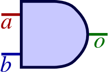 |
AND gate: | Takes two inputs on its left and outputs 1 on its right only if both the first input and the second input are 1 (Figure 2(b)). For the upper AND gate in our example, its upper input is 1 from y, and its lower input is 1 from the upper NOT gate; both inputs are 1, so the AND gate produces 1 as its output. |
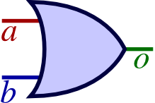 |
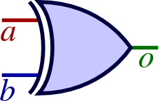
OR gate: | Takes two inputs on its left and outputs 1 on its right if either the first input or the second input are 1 (or if both are 1). (Figure 2(c)) |
Here's a handy mnemonic for distinguishing the shapes for OR and AND: The symbol for the AND gate looks like a capital letter D, which you can find in the word AND.
Figure 2: Logic gate behavior.
(a) NOT gate (b) AND gate (c) OR gate
a o 0 1 1 0
a b o 0 0 0 0 1 0 1 0 0 1 1 1
a b o 0 0 0 0 1 1 1 0 1 1 1 1
After the values filter through the gates based on the behaviors of Figure 2, the values in the circuit will be as follows.
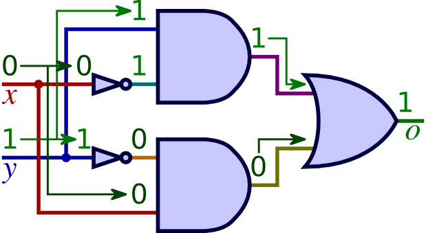
Based on this diagram, we can see that when x is 0 and y is 1, the output o is 1.
By doing the same sort of propagation for other combinations of input values, we can build up the following table showing how this circuit behaves for different combinations of inputs.
x y o 0 0 0 0 1 1 1 0 1 1 1 0
To interpret this table, let's examine the second row: it has a 0 in the x column, 1 in the y column, and 1 in the o column. This indicates that if the x input is 0 and the y input is 1, then the circuit's output o will be 1.
Such a table is called a truth table. A truth table contains a row for every possible combination of input values and each row tells what the value of the circuit's output would be for that combination of inputs. In this example table, we have four rows, representing each possible combination of x and y. Our truth table would have eight rows if the circuit had three inputs; and it would have sixteen if the circuit had four inputs.
2. Building logic circuits
In the previous section, we saw how logic circuits work. This is helpful when you want to understand how a circuit behaves. But computer designers often face the opposite problem: Given a desired behavior, how can we build a circuit behaving that way? Or to ask the same basic question: How can we convert a truth table into a logic circuit?
In this section, we look at a systematic technique for designing circuits. First, though, we'll take a necessary detour through the study of Boolean expressions.
2.1. Boolean expressions
In the middle of the nineteenth century, George Boole designed a system of logic that forms the foundation of the modern computer. He noticed that logical functions could be built from the AND, OR, and NOT operations and that this observation leads one to be able to reason about logic in a mathematical system.
As Boole was working in the nineteenth century, of course, he wasn't thinking about logic circuits. He was examining the field of logic, created for thinking about the validity of philosophical arguments. Philosophers have thought about this subject since the time of Aristotle. Logicians formalized some common mistakes, such as the temptation to conclude that if A implies B, and if B holds, then A must hold also. (“Brilliant people wear glasses, and I wear glasses, so I must be brilliant.”)
As a mathematician, Boole sought a way to encode sentences like this into algebraic expressions, and he invented what we now call Boolean expressions. An example of a Boolean expression is “y x + y x.” A line over a variable (or a larger expression) represents a NOT; for example, the expression y corresponds to feeding y through a NOT gate. Multiplication (as with x y) represents AND. After all, Boole reasoned, the AND truth table (Figure 2(b)) is identical to a multiplication table over 0 and 1. Addition (as with x + y) represents OR. The OR truth table (Figure 2(c)) doesn't match an addition table over 0 and 1 exactly — 1 OR 1 is 1, but 1 plus 1 is 2 — but, Boole decided, it's close enough.
In Boolean expressions, we observe the regular order of operations: Multiplication (AND) comes before addition (OR). Thus, when we write y x + y x, we mean (y x + y x). We can use parentheses when this order of operations isn't what we want. For NOT, the bar over the expression indicates the extent of the expression to which it applies; thus, x + y represents NOT x OR y), while x + y represents (NOT x) OR (NOT y).
A warning: Students new to Boolean expressions frequently try to abbreviate x y as x y — that is, they draw a single line over the whole expression, rather than two separate lines over the two individual pieces. This abbreviation is wrong. The first, x y, translates to (NOT x) AND (NOT y) (that is, both x and y are 0), while x y translates to NOT (x AND y) (that is, x and y aren't both 1). We could draw a truth table comparing the results for these two expressions.
x y x y x y x y x y 0 0 1 1 1 0 1 0 1 1 0 0 0 1 1 0 0 1 0 0 1 1 1 0 0 0 1 0
Since the fifth column (x y) and the seventh column (x y) aren't identical, the two expressions aren't equivalent.
Every expression directly corresponds to a circuit and vice versa. To determine the expression corresponding to a logic circuit, we feed expressions through the circuit just as values propagate through it. Suppose we do this for our circuit of Figure 1.
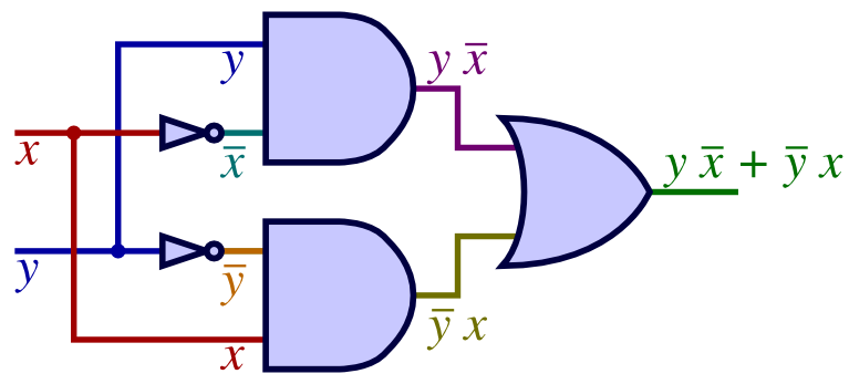
The upper AND gate's inputs are y and x, and so it outputs y x. The lower AND gate outputs y x, and the OR gate combines these two into y x + y x.
2.2. Boolean algebra laws
Boole's system for writing down logical expressions is called Boolean algebra. It's called an algebra because we can manipulate symbols using laws similar to those of traditional algebra. For example, the commutative law applies to both OR and AND. To prove that OR is commutative (that is, that A + B = B + A, we can complete a truth table demonstrating that for each possible combination of A and B, the values of A + B and B + A are identical.
A B A + B B + A 0 0 0 0 0 1 1 1 1 0 1 1 1 1 1 1
Since the third and fourth columns match, we would conclude that A + B = B + A is a universal law.
Since OR (and AND) are commutative, we can freely reorder terms without changing the meaning of the expression. The commutative law of OR would allow us to transform y x + y x into y x + y x, and the commutative law of AND (applied twice) allows us to transform this to x y + x y.
Similarly, OR (and AND) has an associative law (that is, A + (B + C) = (A + B) + C. Because of this associativity, we will free to write A + B + C (and A B C) without parentheses — after all, placing parentheses around the first pair (A + B) results in the same thing as parentheses around the second pair (B + C). In drawing circuits, we'll freely draw AND and OR gates that have several inputs. A 3-input AND gate would actually correspond to two 2-input AND gates when the circuit is actually wired. There are two possible ways to wire this.
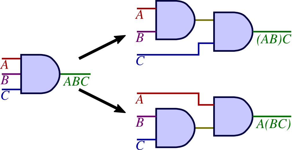
Because of the associative law for AND, it doesn't matter which we choose, and so we'll feel free to ambiguously draw an AND or OR gate with three (or more) inputs.
There are many such laws, summarized in Figure 3. This includes analogues to all of the important algebraic laws dealing with multiplication and addition. There are also many laws that don't hold with addition and multiplication; in the table, these are marked in red with an asterisk.
Figure 3: A sampler of important Boolean identities.
* Those in red with an asterisk don't correspond to standard algebraic identities. AND OR commutative A B = B A A + B = B + A associative A (B C) = (A B) C A + (B + C) = (A + B) + C identity A ⋅ 1 = A A + 0 = A distributive A (B + C) = A B + A C * A + B C = (A + B) (A + C)) one/zero A ⋅ 0 = 0 * A + 1 = 1 idempotency * A A = A * A + A = A inverse * A A = 0 * A + A = 1 DeMorgan's law * A B = A + B * A + B = A B double negation * A = A
2.3. Sum of products
Now we can return to our problem: If we have a particular logical function we want to compute, how can we build a circuit to compute it? We'll begin with a description of the logical function as a truth table. Suppose we start with the following function for which we want a circuit.
x y z o 0 0 0 0 0 0 1 1 0 1 0 1 0 1 1 0 1 0 0 0 1 0 1 0 1 1 0 1 1 1 1 1
Given such a truth table defining a function, we'll build up a Boolean expression representing the function. For each row of the table where the desired output is 1, we describe it as the AND of several factors.
x y z o description 0 0 1 1 x y z 0 1 0 1 x y z 1 1 0 1 x y z 1 1 1 1 x y z
To arrive at a row's description, we choose for each variable either that variable or its negation, depending whether the variable in that row is 1 or not; and then we take the AND of these choices. For example, looking at the first of the rows above, we include x since x is 0 in this row, y since y is also 0, and z since z is 1; our description is the AND of these: x y z. This expression gives 1 for the combination of values on this row; but for other rows, its value is 0, since every other row is different in some variable, and that variable's contribution to the AND would yield 0.
Once we have the descriptions for all rows where the desired output is 1, we observe the following: The value of the desired circuit should be 1 if the inputs correspond to the first 1-row, the second 1-row, the third 1-row, or the fourth 1-row. Thus, we'll combine the expressions describing the rows with an OR:
Note that our expression does not include descriptions for rows where the truth table signals that the desired output is 0: if we did, then that description would be 1, and so the OR of all terms would be 1, not the 0 that we desire.
This expression leads immediately to the circuit of Figure 4.
Figure 4: A circuit derived from a given truth table.
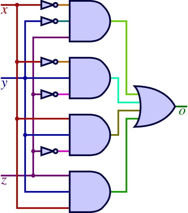
The final expression we get is called a sum of products expression. It is called this because it is the OR (a sum, if we understand OR to be like addition) of several ANDs (products, since AND corresponds to multiplication). We call this technique of building an expression from a truth table the sum of products technique.
This sum of products technique allows us take any function over bits and build a circuit to compute that function. The existence of such a technique proves that circuits can compute any logical function.
To summarize: We have seen three ways of describing a Boolean function: logic circuits, truth tables, and Boolean expressions. Moreover, we have seen systematic ways to convert between the three techniques, diagrammed below.

The only missing arrow is the conversion from truth tables to circuits; we can handle that, though, by converting the truth table to a Boolean expression (using the sum of products technique) and converting that into a circuit.
3. Simplifying circuits
Logic gates are physical devices built using transistors. In practice, the efficiency of a circuit matters. We'll now turn to understanding how to measure a circuit's efficiency, and we'll see a technique that often results in a more efficient circuit than the one we arrive at through using the sum of products technique.
3.1. Measuring circuit efficiency
We can measure a circuit's efficiency in two directions: space and speed. The space factor relates to the fact that each transistor takes up space, and the chip containing the transistors is limited in size, so the number of transistors that fit onto a chip is limited by current technology. Since CPU designers want to fit many features onto the chip, they try to build their circuits with as few transistors as possible to accomplish the tasks needed. To reduce the number of transistors, they try to create circuits with few logic gates. Thus we can approximate the space usage of a circuit simply by counting how many logic gates the circuit includes.
The second factor, speed, relates to the fact that transistors take time to operate. Since designers want circuits to work as quickly as possible, they work to minimize the circuit depth, which is the maximum distance from any input through the circuit to an output. Consider, for example, the two dotted lines in the following circuit, which indicate two different paths from an input to an output in the circuit.
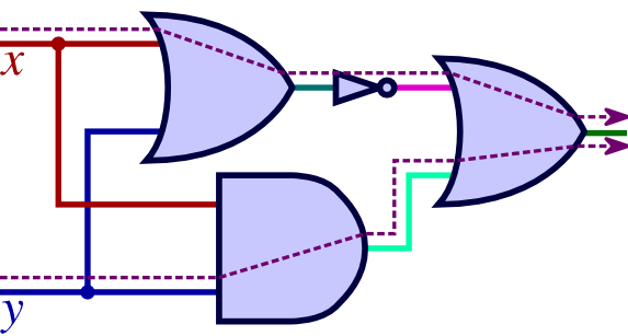
The dotted path starting at x goes through three gates (an OR gate, then a NOT gate, then another OR gate), while the dotted path starting at y goes through only two gates (an AND gate and an OR gate). There are two other paths, too, but none of the paths go through more than three gates. Thus, we would say that this circuit's depth is 3. This is a rough measure of the circuit's speed: Computing an output with this circuit takes about three times the amount of time it takes a single gate to do its work.
The “sum of products technique” that we saw for converting a Boolean function into a circuit isn't too bad using these criteria. The circuit resulting from this technique has a depth of just 3 — or slightly more if you insist (as circuit designers will) that each AND and OR gate has just two inputs. But it does less well than we might hope in terms of space.
3.2. Karnaugh maps
We'll now turn to investigating a technique for building circuits from a truth table, which results in smaller circuits without making any compromises in depth.
For Boolean functions with four or fewer inputs, the Karnaugh map is a particularly convenient way to find the smallest possible sum-of-products expression. It is a simple process: We convert the truth table to a matrix as we'll see later, then we determine how best to “cover” the 1's in the matrix with a set of rectangles; each rectangle will correspond to a term in our sum of products expression.
Let's start with the truth table used in Section 2.3.
x y z o 0 0 0 0 0 0 1 1 0 1 0 1 0 1 1 0 1 0 0 0 1 0 1 0 1 1 0 1 1 1 1 1
Since there are eight rows to this table, we will convert it into a 2×4 matrix. (If there were 4 rows, it would be a 2×2 matrix. And if there were 16 rows, it would be a 4×4 matrix.) One of the variables will be represented along the vertical axis, and the other two variables along the horizontal axis. Note how the variable combinations along the horizontal axis do not go in the traditional order of 00-01-10-11, but instead 00-01-11-10. This is important for the Karnaugh map technique to work.

Having created that matrix, we now fill it by copying the corresponding output values into the appropriate cell. The truth table's last row, for example, maps to the cell in the matrix's second row (since x is 1 in that row of the truth table) and third column (since y and z are both 1 in that row of the truth table). The output in the truth table's last row is a 1, so we place a 1 into that cell of the matrix. Below is the completed matrix, with the 1 corresponding to the truth table's last row circled.

Now we look for the smallest set of rectangular regions that cover all 1's in our table but no 0's. The height and width of each rectangle must be a power of two, so the possibilities are 1×1, 1×2, 1×4, 2×1, 2×2, 2×4, 4×1, 4×2, and 4×4. In our example, we can cover all the 1's using just three rectangles.
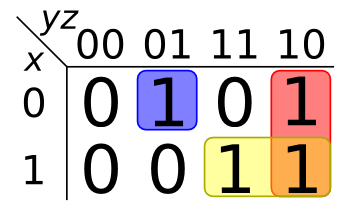
Each of the regions will correspond to a term in a sum of products expression that we build based on the selected regions. The pink region at far right, for instance, under the 10 column, corresponds to the term where y is 1 and z is 0, but x could be either 0 or 1. The corresponding term, then, would be y z. Putting together the terms from the three regions together, we arrive at:
This can be translated into the circuit of Figure 5. Notice how this circuit has only 7 gates in comparison to the 10 gates of Figure 4.
Figure 5: A simplified circuit equivalent to Figure 4.

3.3. A more complex Karnaugh map
Another example will illustrate some additional features of a Karnaugh map. This time, we will work from a truth table over four inputs.
w x y z o 0 0 0 0 1 0 0 0 1 0 0 0 1 0 1 0 0 1 1 0 0 1 0 0 1 0 1 0 1 0 0 1 1 0 1 0 1 1 1 0
w x y z o 1 0 0 0 1 1 0 0 1 0 1 0 1 0 1 1 0 1 1 1 1 1 0 0 0 1 1 0 1 0 1 1 1 0 1 1 1 1 1 1
Since we have 16 rows in this table, we'll start with a 4×4 matrix. Each row will represent a combination of values for the first two variables' values, and each column will represent a combination of the last two variables' values.
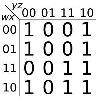
In determining the rectangular regions, we introduce a new rule: Regions can wrap around the edges of the matrix. (This rule applies for three-input functions, too, though it didn't happen to come up in our previous example.) Using this fact, we can cover the 1's using just three rectangles.

The simplest region (drawn in yellow) is in the lower right; it corresponds to the term w y. The upper 2×2 region (drawn in pink) wraps from the last column around to first column; it corresponds to the term w z. There is another region (draw in blue) that wraps between columns and also between rows, so it covers all four corners of the matrix; it corresponds to the term x z. Putting these three terms together, we arrive at our simplified Boolean expression:
When you draw your rectangular regions, you want to use as few as possible: Each region will correspond to an additional AND gate. In our above example, we omitted a possible rectangle that covers the last column, because it wouldn't cover any 1's that weren't already covered.
Moreover, you want each rectangle to cover as many 1's as possible, even if it isn't necessary, because larger rectangles lead to terms containing fewer variables. In our earlier example, we could have drawn the upper pink rectangle as a 1×2 rectangle in the second row only. But then the second terms would have been w x z, which has one more variable in it than we used previously.
4. Other logic gates and universality
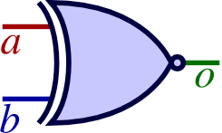
Until now, we've dealt only with AND, OR, and NOT gates. Circuit designers often work with four other gates: NAND (not and), NOR (not or), XOR (exclusive or), and XNOR (not exclusive or). The XOR gate emits 1 when one or the other of its inputs is 1, but not when both are; that is, the case of two 1 inputs is excluded from the situation when the gate emits a 1. The NAND, NOR, and XNOR gates work simply as an AND/OR/XOR gate with a NOT gate after it — and they are drawn as an AND/OR/XOR gate with a small circle at its output. Figure 6 depicts the appearance of these gates and the truth table summaries.
Figure 6: More logic gates.
(a) NAND gate (b) NOR gate (c) XOR gate (d) XNOR gate
a b o 0 0 1 0 1 1 1 0 1 1 1 0
a b o 0 0 1 0 1 0 1 0 0 1 1 0
a b o 0 0 0 0 1 1 1 0 1 1 1 0
a b o 0 0 1 0 1 0 1 0 0 1 1 1

We haven't looked at these gates previously because they can all be built using AND, OR, and NOT gates. In fact, we've seen that every truth table has a circuit of AND, OR, and NOT gates that corresponds to it — we simply derive the sum of products expression (which has only AND, OR, and NOT operations) and then build the corresponding circuit. Because of this property, we call the combination of AND, OR, and NOT universal.
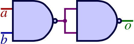
Somewhat more surprising is that the NAND gate alone is universal — that is, any truth table can be implemented by a circuit that includes only NAND gates. To convince ourselves of this, we start with the fact that any truth table can be implemented using AND, OR, and NOT gates; and then we see how one can replace each AND/OR/NOT gate with a system of NAND gates to arrive at a circuit including only NAND gates. Figure 7 demonstrates the NAND-gate system corresponding to each of AND, OR, and NOT.
Figure 7: Building NOT, AND, and OR using NAND gates.
is converted to is converted to is converted to

We can do a similar thing to find that NOR gates by themselves are universal.
The fact that NAND is universal is often used by circuit designers. Though designers at first design a circuit using AND, OR, and NOT gates, in practice circuits are easier to manufacture when they use only NAND gates (or only NOR gates). (Why this is so is not something we'll tackle here.) Thus, their initial AND/OR/NOT designs are converted to use only NANDs (or NORs).
In any case, by this point we have seen how you can build up a reasonably small circuit for any possible logical function. This knowledge forms the basis for building up full computational devices.